Skip the schematic.
Draw the board.
Free PCB layout editor for makers — iPhone, iPad, Android & web
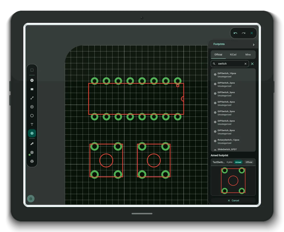
A PCB editor for people who would rather be soldering. Place footprints, route copper pad to pad, and run a Design Rule Check before you commit. Then print a mirrored 1:1 mask and etch the board tonight — or send Gerbers to a fab.
Sign in with Google — no credit card, nothing to install. Etching masks are free on every plan; Gerber export is on Engineer.
Everything a prototype needs. Nothing it doesn't.
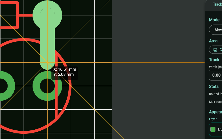
WYSIWYG Layout Editor
See exactly what you'll get. Place footprints, route copper traces, and arrange your board visually — what you see on screen is what gets fabricated. No netlist required.
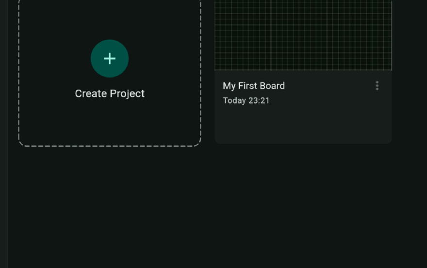
Cloud Project Sync
Your projects are backed up and synced across your devices — like Dropbox for your PCBs. Pick up on your phone where you left off on the web, always with the latest version.
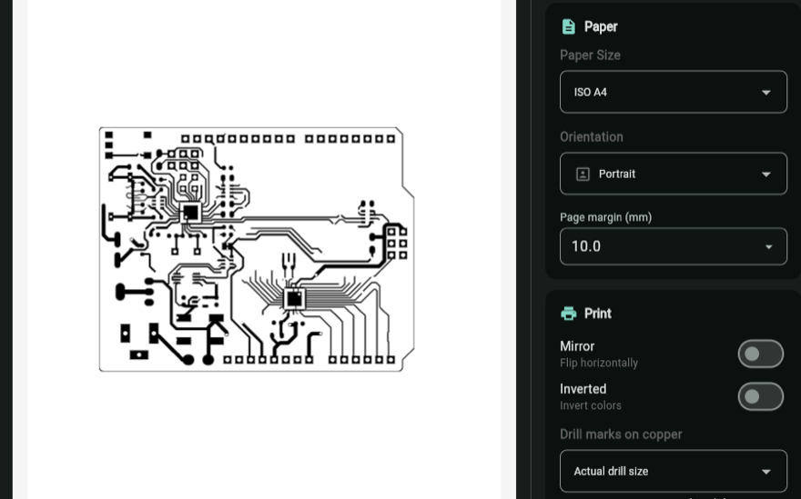
Gerber & PDF Export
Export Gerber files to send straight to a PCB fab, or generate a PDF to etch your own board at home. Either way, you're one tap away from something physical.
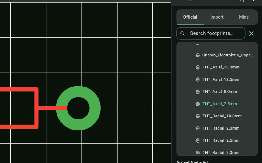
Rich Footprint Library
Start with a built-in component library, import footprints from KiCad, or add any public GitHub repository as a footprint source. Your parts, your workflow.
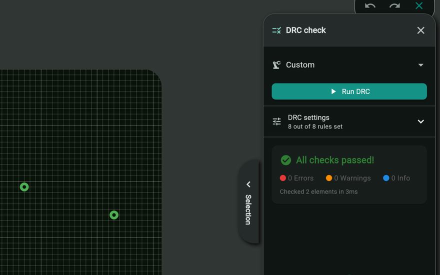
Design Rule Check
Catch shorts, clearance violations, and unconnected copper before you order. DRC runs right in the editor and points at every problem on the board.
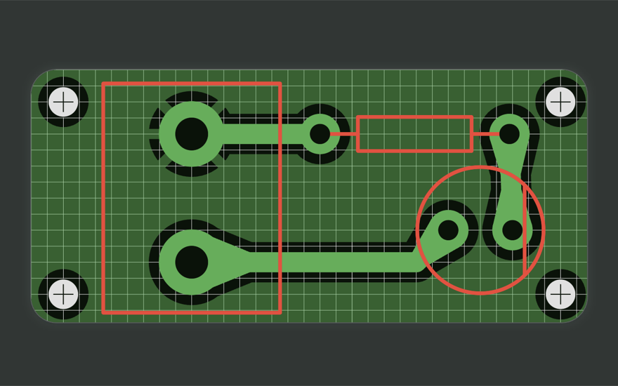
Ground Pours & AutoGround
Fill copper areas with a tap. AutoGround pours the ground plane around your traces and keeps it up to date as your layout changes.
The fiddly parts, generated.
A spiral inductor, a grid of forty vias, mounting holes that actually line up with an Arduino — tedious to draw and easy to get wrong. Open Insert, answer a few questions, and finished geometry lands on the board.
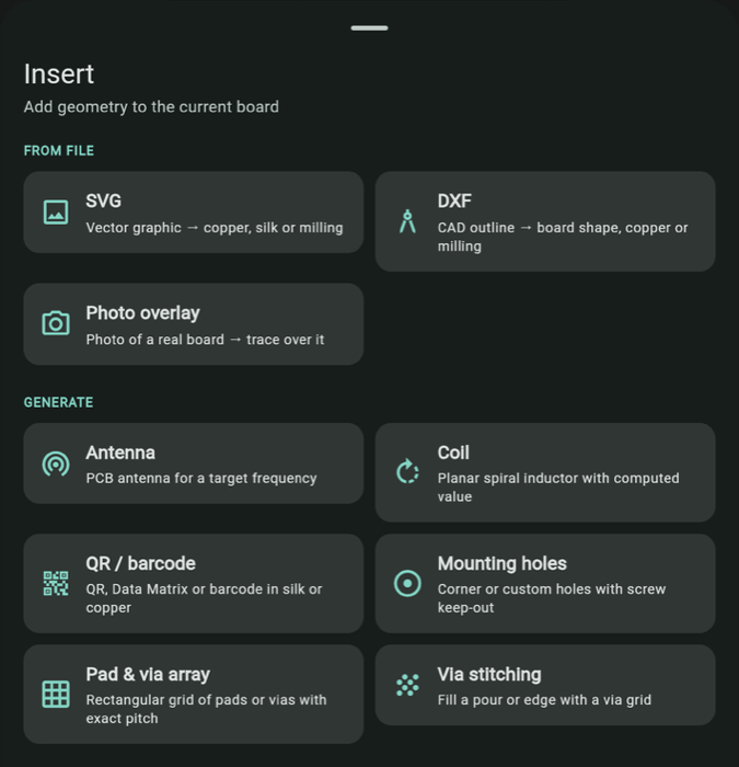
Generate
From file
On any pad or track
Every generator is fully usable before you pay — configure it, see the live preview, and read the computed values. The plan is only needed to drop the result onto your board.
Bring your projects with you.
Sprint Layout
Open .lay6 files as full projects — boards, traces, pads and all — and import .lmk macros into your library. Design on from where Sprint Layout left off, now on iPhone, iPad, Android and the web. How to import .lay6 files →
KiCad
Open .kicad_pcb boards as full projects, free on every plan — the layout comes across and you keep working on it here. Pull in .kicad_mod footprints and whole libraries too, from local files or straight from GitHub. How to import from KiCad →
Eagle
Open your .brd board files as full projects — the layout you built in Eagle comes across so you can keep working on it here, on any device you own. How to import .brd files →
Opening Sprint Layout, KiCad and Eagle boards as new projects is free on every plan — we never gate the way in; only the cloud-board limit applies. Importing footprints and macros into your reusable library starts with the Maker plan.
From idea to board in three steps.
Place components
Search the built-in footprint library, import from KiCad, or pull footprints from any public GitHub repo — then drag parts straight onto the board.
Route your traces
Draw copper pad-to-pad, pour ground planes with AutoGround, and let the Design Rule Check flag shorts and clearance issues as you go.
Export & build
Export Gerber files any PCB fab accepts, or a mirrored PDF mask to etch the board at home. Your design becomes a real board.
New to PCB design? Read the step-by-step guide to your first board →
Not another heavy EDA suite — a KiCad alternative built for simplicity
Unlike KiCad, Eagle, Fritzing, or Altium — Protoboard Designer is designed to get you from idea to board in minutes, not days.
"The GOAT of Android PCB designers."
"Surprisingly flexible and intuitive… AutoGround is really well done."
Free to start. Upgrade when you outgrow it.
Subscriptions are billed through the App Store or Google Play and sync automatically to the web app. Prices shown in USD — your local price and any current offer appear at checkout.
Free
$0 forever
Everything you need for your first boards
- Full layout editor & Design Rule Check
- Mirrored 1:1 PDF masks — everything home etching needs
- 3 cloud-synced boards
- Built-in footprint library + 5 of your own
- Open Sprint Layout, KiCad & Eagle boards
- PDF & image export, watermarked
Maker
$5.99 / month
For hobbyists building their own boards
- Everything in Free
- Up to 20 cloud boards
- Unlimited custom macros
- Turn the watermark off
- Mosaic printing — several copies per sheet, so film isn't wasted
- KiCad footprint libraries & Sprint Layout macros
Engineer
$10.99 / month
For professionals and power users
- Everything in Maker
- Unlimited boards
- Gerber export — send straight to any fab
- Thermal pads
- Watermark-free exports by default
Frequently asked questions
Is Protoboard Designer free?
Yes. The free plan includes the full layout editor, Design Rule Check, 3 cloud-synced boards, 5 custom footprints, mirrored 1:1 PDF masks for home etching, and free import of Sprint Layout, KiCad and Eagle boards — no credit card required. Optional Maker and Engineer plans unlock more boards, footprint-library import, mosaic printing, watermark-free exports, and Gerber export.
Is Protoboard Designer an online PCB editor?
Yes. Protoboard Designer runs entirely in your browser as a WebAssembly web app — there's nothing to install. It's a full online PCB editor: design boards, route copper, run a Design Rule Check, and export Gerber or PDF files. The same editor is also available as an iPhone, iPad and Android app, and your projects sync between them.
Do I need EDA or PCB design experience?
No. Protoboard Designer is a WYSIWYG editor: you place footprints and draw copper traces directly on the board — no schematic or netlist required. What you see on screen is what gets fabricated.
Can I import KiCad footprints?
Yes — and whole boards too. Opening a .kicad_pcb board as a new project is free on every plan. Importing .kicad_mod footprints and whole libraries into your reusable library — including from any public GitHub repository — is part of the Maker plan.
Can I open my existing Sprint Layout, KiCad, or Eagle designs?
Yes. Sprint Layout .lay6, Eagle .brd and KiCad .kicad_pcb files all open as new projects — traces and pads included — free on every plan. We don't gate the way in; the only limit for free users is the number of cloud boards. Importing reusable footprint libraries (.kicad_mod, including straight from GitHub) and Sprint Layout .lmk macros starts with the Maker plan.
Can I order my board from JLCPCB, PCBWay, or another fab?
Yes. Protoboard Designer exports industry-standard Gerber files (Engineer plan) that any PCB manufacturer — JLCPCB, PCBWay, OSH Park, Aisler, and others — accepts directly.
Can I etch a PCB at home with it?
Yes, on the free plan. Export your layout as a PDF mask — mirrored for toner transfer or photoresist — print it at 1:1 scale, and etch the board at home. Mirroring is free on every plan. Maker adds mosaic printing, which fits several copies of the same board on one sheet — so a sheet of transfer film or photoresist gives you spares instead of one board.
Does it work on my phone or tablet?
Yes. The full editor runs on iPhone and iPad, on Android phones and tablets via the Google Play app, and in any modern desktop browser as a WebAssembly web app. Projects sync between devices automatically.
Is there an iOS app?
Yes. Protoboard Designer is on the App Store for iPhone and iPad, and needs iOS 15 or later. It's the same editor as the Android and web versions, and your projects sync between all of them — so you can lay a board out on an iPad and pick it up on your desktop. If you'd rather not install anything, the web app still works in Safari.
How is it different from KiCad or Fritzing?
KiCad is a full schematic-driven EDA suite — powerful, but with a steep learning curve. Fritzing focuses on breadboard diagrams. Protoboard Designer sits in between: a direct, visual PCB layout editor that gets you from idea to a fabricatable board in minutes, on whatever device you have to hand. For complex multi-sheet schematic projects, a full EDA suite is still the right tool.
Your next circuit starts here.
No credit card required. Open the web app in your browser, or install it on iPhone, iPad or Android — your boards sync across all of them. Start laying out your board in seconds.