How to Export Gerber Files in Protoboard Designer
Estimated reading time: 6 minutes
Gerber files (the standard PCB fabrication format) describe each layer of your board as vector data a factory can etch, drill, and print. Manufacturers such as JLCPCB, PCBWay, and OSH Park accept Gerber uploads every day. This guide walks you through export inside Protoboard Designer and how to send the zip to a fabricator.
Make sure:
- Your board is the right size (the outline is exported automatically — every board has a closed edge)
- All traces are connected (no floating pads)
- You have reviewed your layout in the visual preview
What Are Gerber Files?
Gerber files tell a fabricator exactly where copper, solder mask, silkscreen, and the board outline should appear. You can think of them as a stack of transparent films—one film per layer—that the shop lines up before etching and drilling.
One export job usually creates multiple Gerber files (often one file per layer) plus a separate drill file. You zip those files together so the manufacturer receives every layer in a single upload.
You don't need a separate step for the board edge. Every board has a closed outline (it starts as a rectangle), and Protoboard Designer includes that outline file in the Gerber export for you — there's nothing to draw or remember. The same outline is also available as an option when you export a PDF.
| File | Layer | What it contains |
|---|---|---|
| copper_top.gbr | C1 - Copper Top | Top copper traces and pads |
| copper_bottom.gbr | C2 - Copper Bottom | Bottom copper traces |
| silkscreen_top.gbr | S1 - Silkscreen Top | Component labels |
| outline.gbr | O - Outline | Board shape and cutouts |
| drill.drl | Excellon | All drill hole positions and sizes |
Export Steps
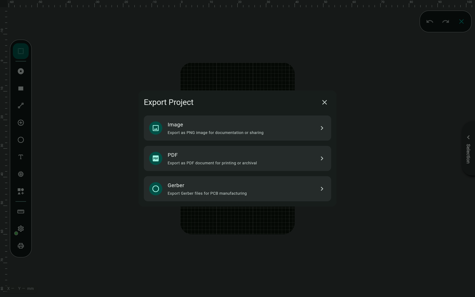
- Open the Export tool from the left toolbar, then choose Export Gerber Files to open the export dialog.
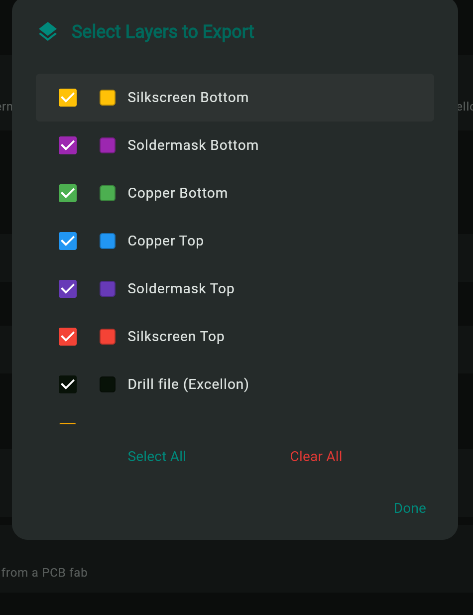
- In the export dialog, review the list of layers and place a check next to each layer you need—at minimum include C1, C2, S1, and O for a typical two-layer board.
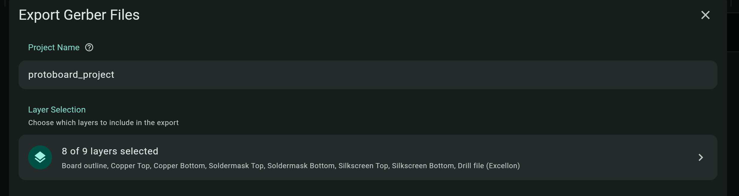
- Set the output filename or project name field so the zip uses a clear label (for example
my-led-board).
- Click Create Gerber Files (or Generate, if the button uses that label) and wait until the progress indicator finishes.
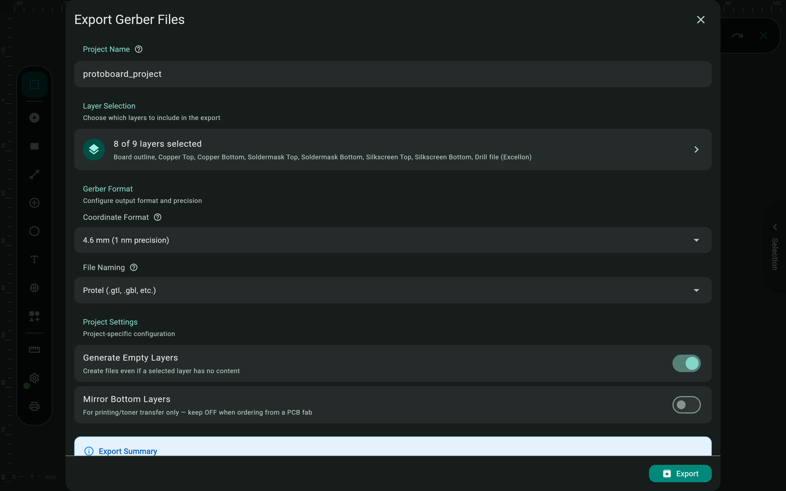
- When the browser or system prompts you, choose Download (or Save) and store the
.zipin a folder you will upload to the fabricator.

- Open the zip locally and confirm you see files such as
copper_top.gbr,copper_bottom.gbr,silkscreen_top.gbr,outline.gbr, anddrill.drl(names may vary slightly with your settings).

For a standard 2-layer board: C1, C2, S1, and O are the minimum. Always include the drill file (Excellon export). Check with your manufacturer if unsure—most publish a supported formats page.
Sending Files to a Manufacturer
JLCPCB: Create an account, start a new PCB order, upload your .zip when the site asks for Gerber files, then follow the preview wizard to confirm layer mapping and board size before you pay.
PCBWay and OSH Park follow the same general idea: upload the zip, review the automated preview, then continue to checkout. Many shops accept the archive directly without asking you to split layers by hand.
Troubleshooting
My manufacturer says the files are invalid
This is usually a file-extension or layer-mapping mismatch, not a missing outline (the outline is always exported for you). Confirm every layer you need was included in the export, and match the file extensions your fabricator lists on its upload help page.
I don't see my traces in the Gerber preview
Re-export and verify you checked C1 and C2 during export. If either copper layer stays unchecked, the preview will look empty on that side.
The board outline is wrong
The board edge comes from your board shape, not from copper you draw. Check its size and shape in Board Settings and with the Machining tool (Outline mode), and make sure any custom shape doesn't cross itself.
Drill holes are missing
The drill file is a separate Excellon export. If you only inspect copper Gerber files, you will not see plated holes until you load drill.drl (or the equivalent name) in your viewer or the fab portal.