Generate Antennas, Coils, QR Codes & More (Insert Hub)
Estimated reading time: 5 minutes
Some board features are tedious to draw and easy to get wrong — a spiral inductor, a grid of 40 vias, mounting holes that actually match an Arduino. The Insert Hub generates them for you, parametrically. Open the Insert tool on the left toolbar and pick a tile; every generator asks a few questions and drops finished geometry onto the board.
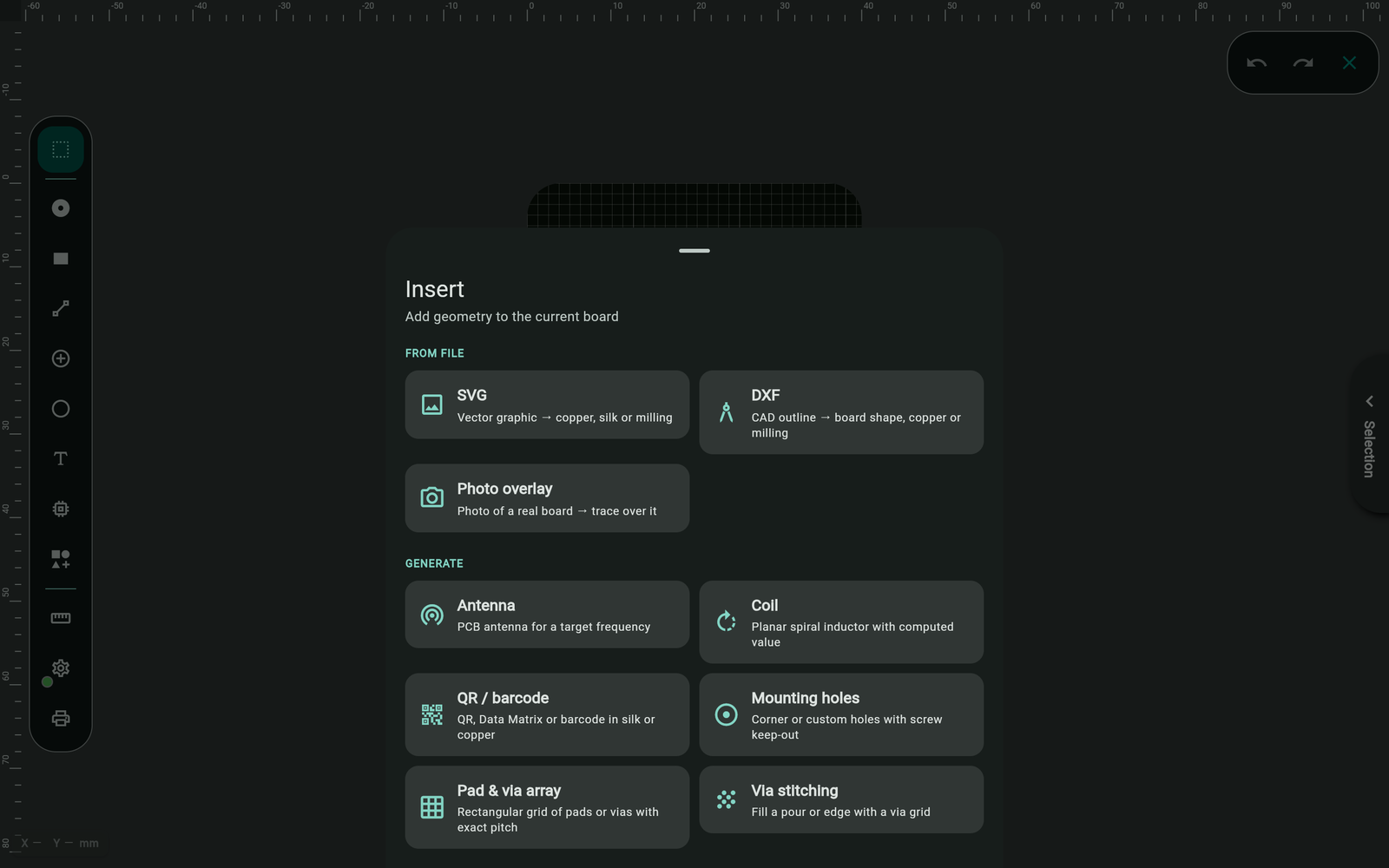
Generate
Antenna
Generates a PCB antenna for a target frequency — enter the frequency and the generator produces the copper structure, ready to place. A serious time-saver for ISM-band projects (433 MHz, 868/915 MHz, 2.4 GHz) where hand-drawing an antenna is guesswork.
Coil
Draws a planar spiral inductor and computes its value from the geometry — turns, spacing, and size in, inductance out. Use it for wireless charging experiments, NFC, or wherever a wound part should become copper.
QR / barcode
Renders a QR code, Data Matrix, or barcode in silkscreen or copper — link the physical board to its repo, docs, or serial number. Scannable straight off the board.
Mounting holes
Adds corner or custom mounting holes with screw keep-outs, including presets for common form factors — Arduino Uno R3, Raspberry Pi HAT, Adafruit Feather — so your board bolts onto real hardware the first time.
Pad & via array
Generates a rectangular grid of pads or vias at an exact pitch. Headers, test-point fields, prototyping grids — anything repetitive.
Breakout / adapter
Fans a fine-pitch SMD part out to a 0.1″ header — the classic breakout board, generated instead of hand-routed.
Via stitching
Fills a pour or board edge with a grid of vias — the standard technique for tying top and bottom ground planes together and taming EMI on two-layer boards.
From file
- SVG — import vector artwork onto copper, silkscreen, or milling. Logos, ornamental copper, unusual outlines: draw in Inkscape, import here, at real size.
- DXF — bring a CAD outline in as the board shape, copper, or milling. Perfect when the enclosure came first and the board must fit it.
- Image (PNG/JPG) — marked Soon: raster logo → silkscreen is on the roadmap. Until then, trace it to SVG and import that.
The SVG/DXF importers are unit-aware and import at true dimensions — measure once in your CAD tool and the board matches.
Troubleshooting
My SVG imports but looks wrong
Complex SVG features (filters, gradients, text-as-text) don't map to copper. Convert text to paths and flatten effects in your vector editor, then re-import.
The generated antenna/coil value isn't what I measured
Generators compute from ideal geometry; nearby copper, the board stack-up, and enclosures shift real-world values. Treat the output as a strong starting point and validate critical RF designs by measurement.
- Define Your Board Shape — pairs well with DXF outlines
- Add a Ground Pour — then stitch it with vias
- PCB Basics: the toolbar at a glance