Design Your First PCB in 5 Minutes
Estimated reading time: 4 minutes
Protoboard Designer is a free-to-start, browser-based printed circuit board (PCB) layout editor — open it at https://app.protoboarddesigner.com. This guide is for complete beginners: no electronic design automation (EDA) experience needed. In five short steps you'll place two parts, connect them with copper, and end up with a layout you could actually manufacture.
A resistor and an LED, placed and routed. It's deliberately tiny — two parts is exactly enough to learn placing, routing, and saving. (A usable board would also need a power connector; that's the natural next step once you know the moves.)
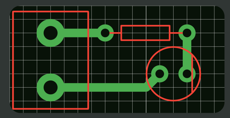
Step 1 — Create a project and size the board
- Open https://app.protoboarddesigner.com in a desktop browser (or launch the Android app).
- Choose Create Project, give it a title, and confirm. The editor opens with a default-sized board.
- Open Board Settings (gear icon, left toolbar) → Board Dimensions and set 50 × 50 mm.
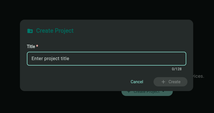
Designing starts with a free account — sign in with Google, no credit card. That's what gives you cloud-synced boards, custom footprints and exports. Details in Projects, Cloud Sync & Backups.
A smaller board keeps parts close together, so you spend your time designing instead of panning around. You can resize the board at any point — the design stays put.
Step 2 — Place a resistor
A footprint is the pattern of copper pads and silkscreen that matches a real part. You don't draw parts — you place footprints from the library:
- Open the Footprints tool from the left toolbar.
- In the Official tab, search for axial (the classic through-hole resistor shape) and pick one — THT_Axial_7.5mm fits a standard ¼ W resistor.
- Tapping the footprint arms it — you'll see it in the Armed footprint preview at the bottom of the panel.
- Press Placement, then tap the board where you want the part. It snaps to the grid.
- Placement stays armed so you could stamp several in a row; switch back to the Selection tool when you're done.
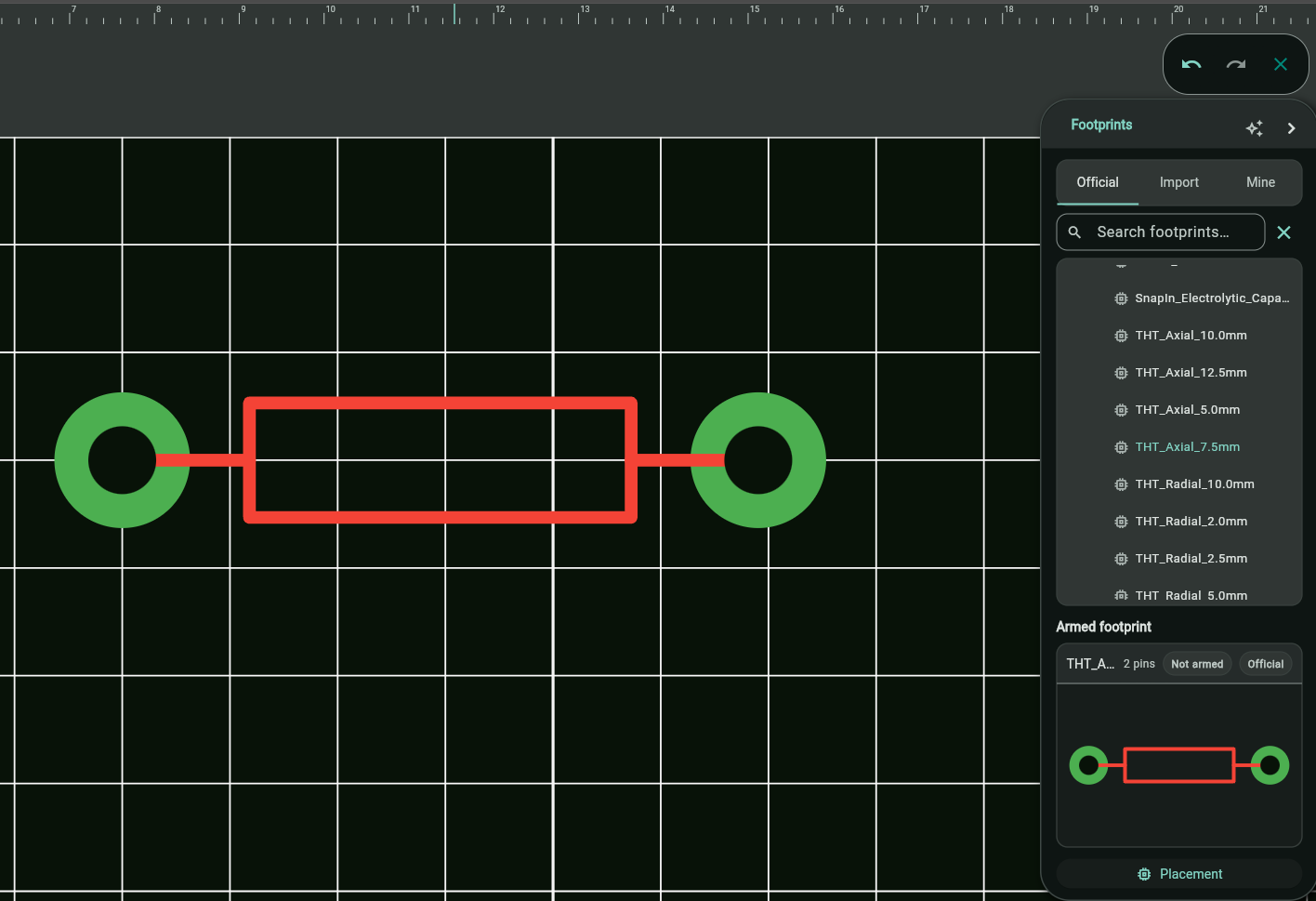
Select it with the Selection tool and drag to move, or grab the rotation handle next to the selection to spin it (it snaps in clean steps). Undo fixes anything. You can't break a board by exploring.
Step 3 — Place an LED
Same moves, second part:
- In the Footprints tool, search for LED.
- Pick a through-hole LED — LED_THT_5mm is the classic 5 mm dome.
- Arm it, press Placement, and tap the board a couple of grid squares from the resistor, so there's room to route between them.
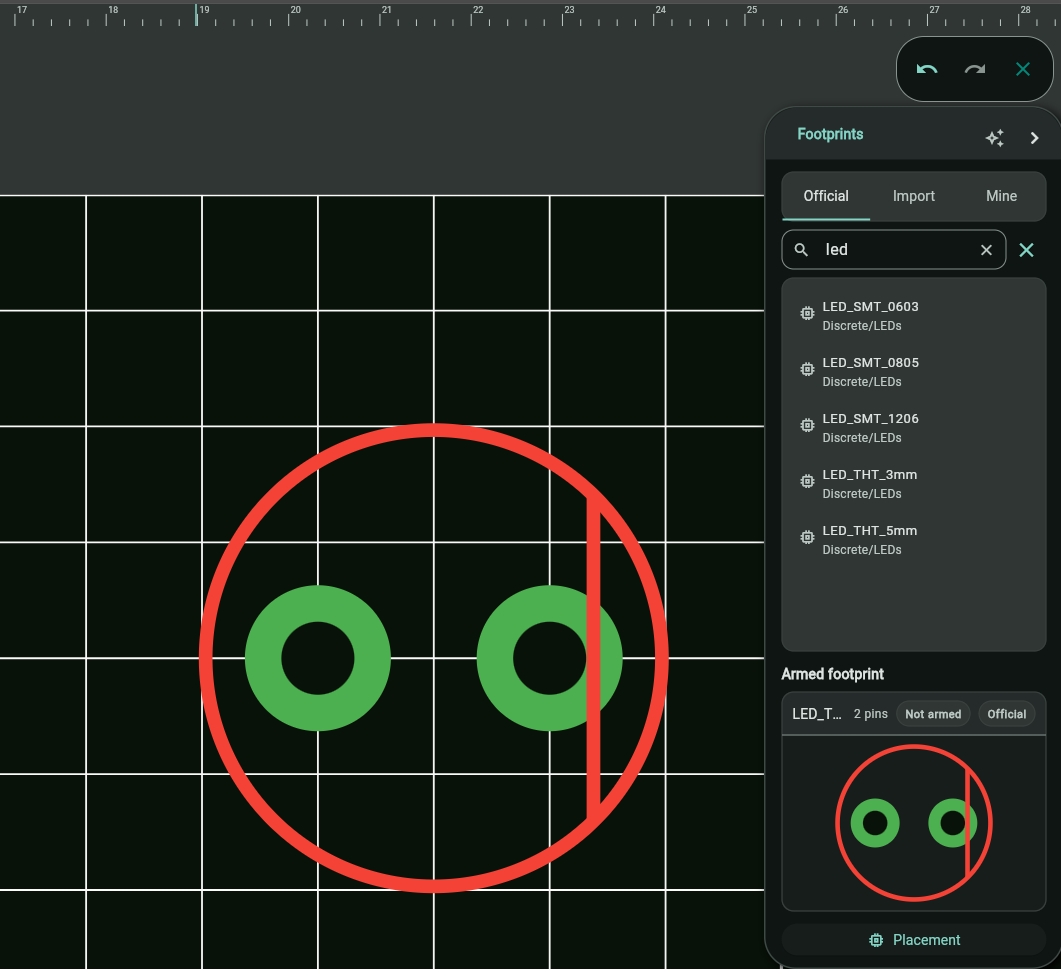
Many footprints mark pin 1 with a square pad while the rest are round. That's your orientation reference — for a real LED, match it against the datasheet so the part doesn't go in backwards.
Step 4 — Route a copper trace
Now connect the parts with copper:
- Select the Track tool from the left toolbar.
- In its panel, check two things: the layer you're drawing on (each copper layer has its own colour) and the track width — the panel even shows the maximum current that width can carry.
- Click a resistor pad to start, then click an LED pad to finish. Add clicks at grid points in between to steer the trace around obstacles.
- Press Esc or switch to the Selection tool when you're done.
What you just drew is exactly what gets etched — WYSIWYG: the copper on screen is the copper on the finished board.
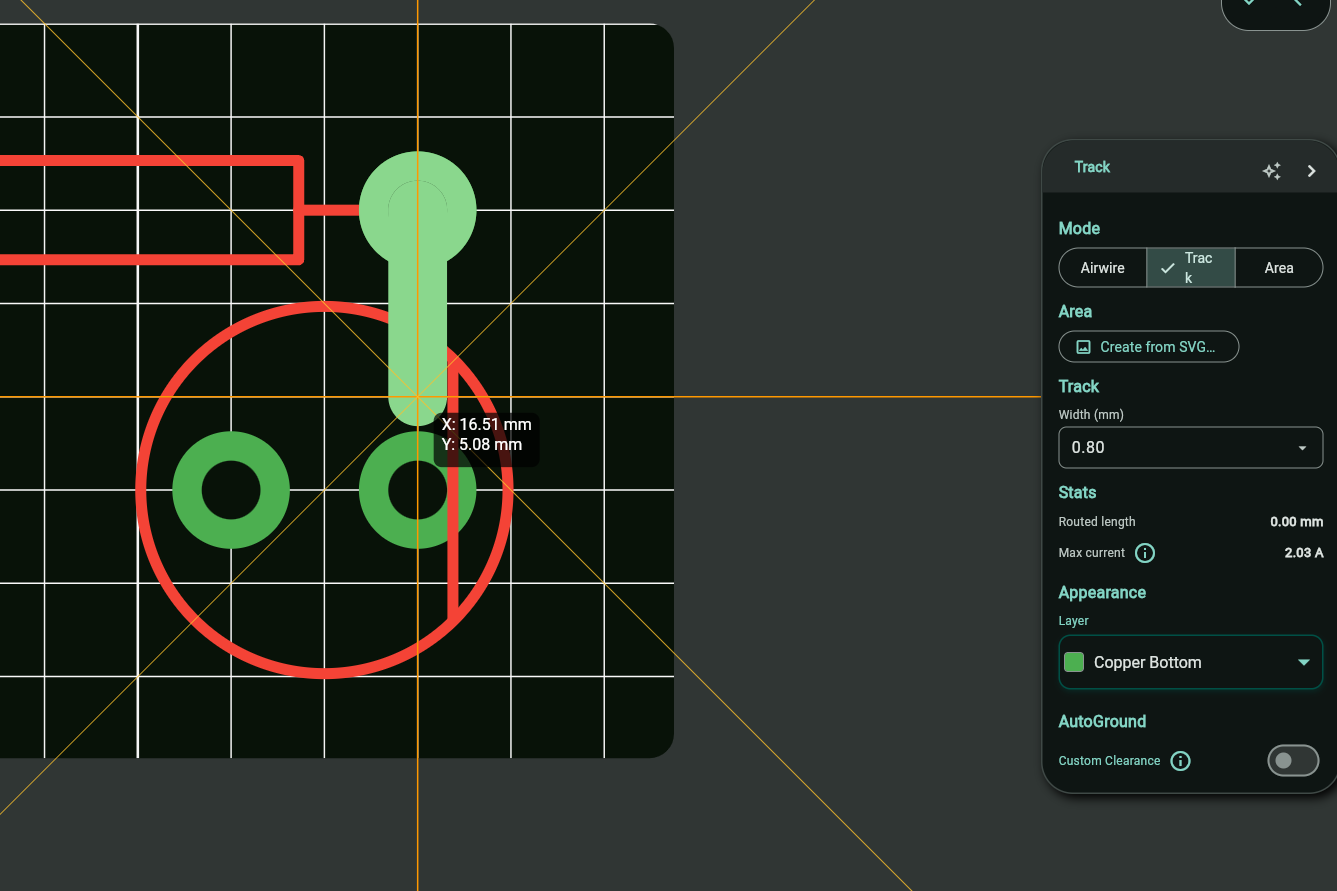
On a real project you can declare connections first as airwires (a visual to-do list) and let autoroute draw the copper — see Connect Components and Route Traces.
Step 5 — Keep it: sign in and sync
If you're signed in, there's nothing to do — your board saves and syncs to the cloud automatically while you edit, and the same project opens on the web and Android.
- Not signed in yet? Open the account menu and sign in (a free account is enough) — the app keeps the board you just made.
- To see sync in action, open the app on another device: your board is waiting under Cloud in the project list.
Projects in your Local list live only on that device and need no account. Cloud projects follow you everywhere. There's no in-editor sync indicator yet — the project list on a second device is the way to confirm a board synced. More in Projects, Cloud Sync & Backups.
Make it real
That's the whole core loop: place → route → save. Everything else is refinement of those three moves. When a design is worth manufacturing:
- Run the Design Rule Check — it catches anything a factory can't build, before you pay for it.
- Export Gerber files and order the board from any fab for a few dollars — or print a PDF mask and etch it at home tonight.
- Find Your Way Around the Editor — grid, layers, selection: five minutes that pay off forever
- PCB Basics: Terms Every Beginner Should Know
- Choosing Trace Width & Spacing
- Import KiCad footprints — thousands of ready-made parts