How to Check Your Design with DRC
Estimated reading time: 6 minutes
Before you spend money on a board, run the Design Rule Check (DRC). It scans your layout for things a factory can't reliably make — traces too thin, copper too close, holes too small, parts hanging off the edge — so you fix them on screen instead of discovering them in a failed batch. Think of it as spell-check for your PCB.
Make a clean DRC the last step before you export Gerbers. A two-minute check saves a wasted order.
Run the check
- Open the Net Probe tool from the left toolbar.
- Choose Run DRC check.
- Review the list of issues. Each one points to the rule it broke; open its rule info for details.
Fix the flagged items, re-run, and repeat until it's clean.
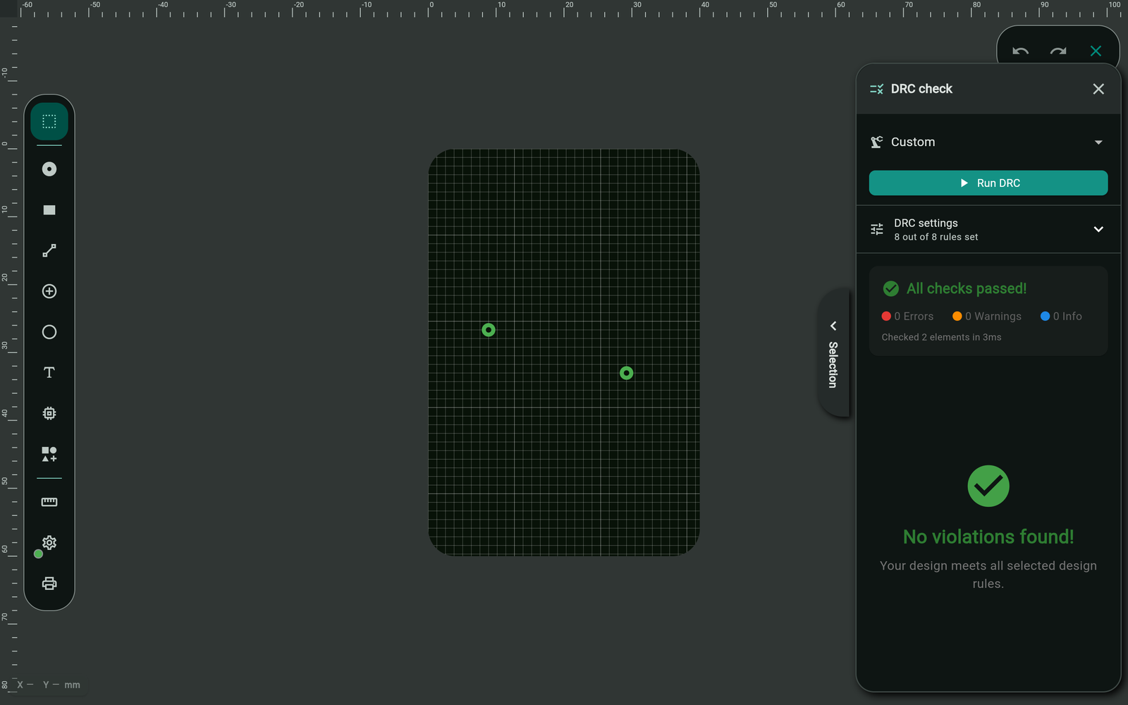
In DRC settings you can enable/disable individual rules and set their thresholds (minimum trace width, clearance, drill size, and so on). Match them to your manufacturer's published capabilities so the check reflects what your shop can actually build.
What the rules check
The DRC covers the common manufacturability and reliability traps. Grouped by area:
Copper
- Minimum trace width — no trace is thinner than allowed (thin copper is fragile and hard to etch). Fix: widen the trace.
- Minimum trace spacing / Copper clearance — separate copper stays far enough apart to avoid shorts and etching defects (measured edge-to-edge, not centre-to-centre). Fix: move copper apart or raise the pour clearance.
- Minimum annular ring — enough copper collar around a drilled hole so the drill can't break out of the pad. Fix: bigger pad or smaller drill.
Drills
- Minimum drill size — holes aren't smaller than the fab can drill. Fix: enlarge the hole.
- Maximum drill size — holes aren't unreasonably large for a drilled hole (use a routed slot instead). Fix: shrink the hole or switch to a slot.
- Minimum drill spacing — holes aren't so close they'd break the material between them. Fix: space them out.
- Drilling on SMD pad — catches a drill accidentally placed on a surface-mount pad. Fix: remove the drill or use a through-hole pad.
Pads
- Minimum pad size — pads are big enough to solder reliably. Fix: enlarge the pad.
- Pad overlap — pad copper areas don't overlap (a short/soldering hazard). Fix: separate the pads.
- Pads without soldermask opening — solderable pads actually have a mask opening. Fix: enable the soldermask opening.
Silkscreen & soldermask
- Minimum silkscreen track width — printed lines aren't too thin to render. Fix: thicken the silk.
- Silkscreen over pads — labels aren't printed on pads (it interferes with soldering). Fix: move the text off the pad.
- Soldermask out of pads — mask openings line up with pads. Fix: correct the opening.
Board
- Elements outside board outline — every pad, track, via, and hole sits inside the board edge. Fix: move it inside, or enlarge the board (see Define Your Board Shape).
Some checks (like copper clearance and pad overlap) can optionally exempt same-net copper, since two things on the same connection touching on purpose isn't a short. If a "violation" is actually intended same-net copper, that's expected — confirm it's the same net.
Quick checklist
- Run Net Probe → Run DRC check before every export.
- Open rule info on anything you don't understand.
- Set thresholds in DRC settings to match your fab.
- Re-run until the list is clean.
Troubleshooting
I have a flood of warnings
Your thresholds may be stricter than your design or your fab needs. Open DRC settings and set each rule to your manufacturer's published minimums, then re-run.
A clearance warning looks wrong — those nets touch on purpose
If the two pieces of copper are on the same net, that's intended. Enable the same-net exemption where available, and verify they really are the same connection.
Parts are flagged as outside the board
The board outline is too small or the element is misplaced. Move it inside the edge, or enlarge the outline in Board Settings → Board Dimensions.