How to Add a Ground Pour (Copper Fill)
Estimated reading time: 5 minutes
A ground pour (or ground plane) is a large area of copper tied to ground that fills the empty space on a layer. It makes wiring ground trivial, lowers noise, and is standard practice on almost every real board. Protoboard Designer can generate one for you automatically with AutoGround — it fills the board and flows around your components and traces, keeping a safe clearance.
It pours copper into the free space on a layer, automatically avoiding your pads, tracks, vias, and other elements by a clearance you set. No drawing required.
Turn on AutoGround
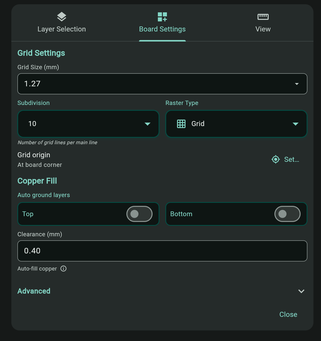
- Open the Board Settings tool from the left toolbar.
- Find the Copper Fill section.
- Enable Copper Top AutoGround and/or Copper Bottom AutoGround for the layer(s) you want filled.
- Set the AutoGround clearance — the gap the pour keeps from every copper feature. 0.4 mm is a sensible default (the range is roughly 0.1–5.0 mm).
The pour appears immediately and updates live as you add, move, or delete elements.
The AutoGround clearance doubles as copper-to-pour spacing. Keep it at least as large as your manufacturer's minimum spacing (often 0.15–0.2 mm) so the board is manufacturable. When in doubt, 0.4 mm is safe and cheap.
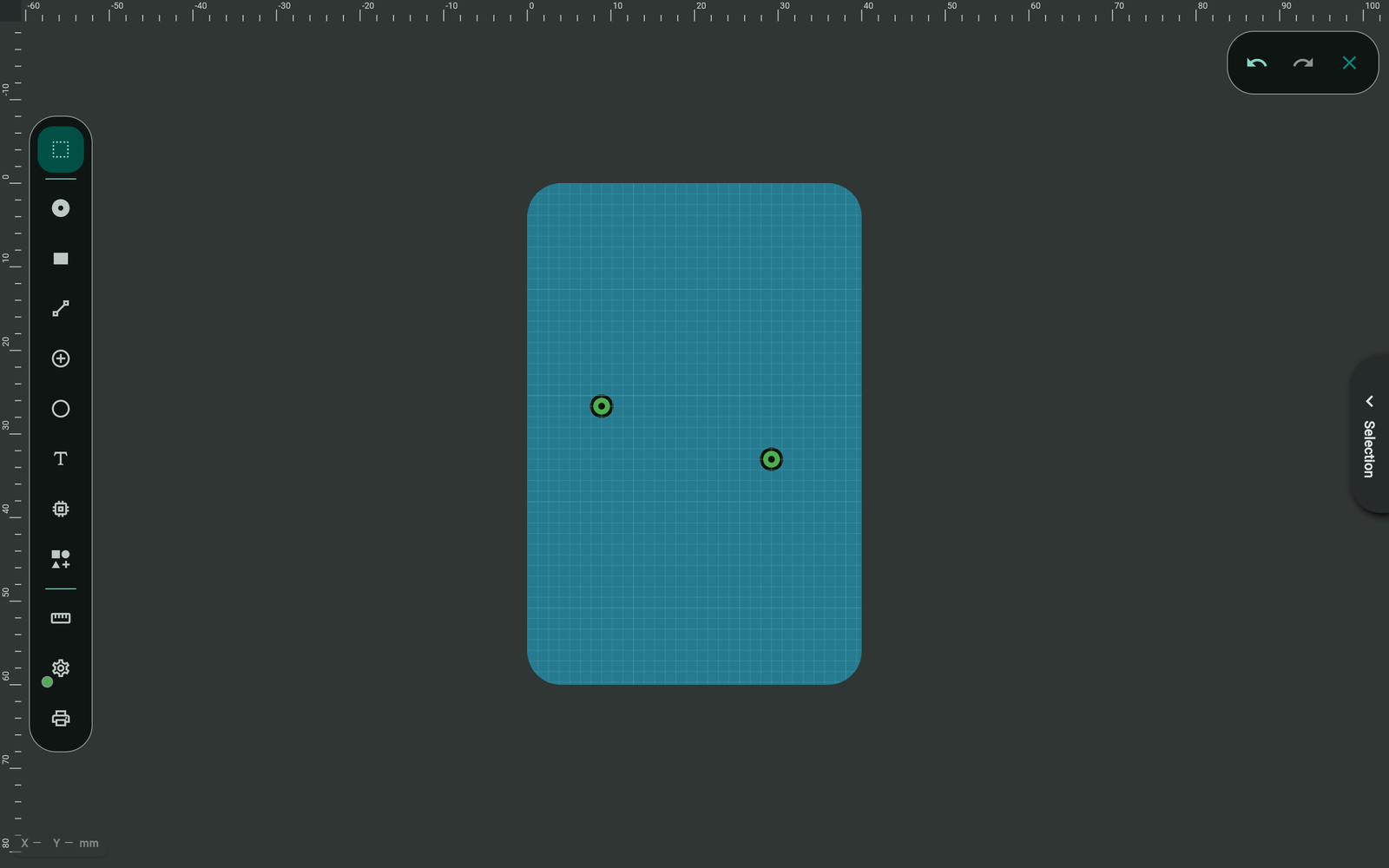
Fine-tune clearance per element
Most elements use the global clearance, but you can override it on a single pad, track, via, label, or circle — useful when one part needs a little more breathing room from the pour. Look for the custom clearance option in that element's properties; when it's off, the element uses the global AutoGround clearance.
Connecting pads to the pour
A pad sitting inside the pour can be joined to it with thermal relief (a thermal pad) — short copper "spokes" that connect the pad to the surrounding AutoGround copper while keeping it easy to solder. Use this for the pads you actually want grounded.
A pour flows around copper by default. A pad only joins the ground if it's connected to it (e.g. via a thermal pad). Don't assume a pad is grounded just because copper surrounds it — confirm the connection.
After pouring: check it
Run the DRC once your pour is in place. The Copper clearance rule confirms the pour keeps its distance from every other copper feature, and the check respects thermal reliefs. See Check Your Design with DRC.
Quick checklist
- Board Settings → Copper Fill → enable AutoGround for the layer(s).
- Set a clearance ≥ your fab's minimum (0.4 mm is a safe default).
- Connect the pads you want grounded (thermal relief).
- Run DRC to confirm clearances.
Troubleshooting
The pour isn't showing up
Confirm AutoGround is enabled for that layer in Board Settings → Copper Fill, and that the layer's visibility is on in the Layer Selector.
The pour crowds my traces
Raise the AutoGround clearance, or set a larger custom clearance on the specific elements that need more room.
A pad I wanted grounded isn't connected
Surrounding copper doesn't mean connection. Add thermal relief (a thermal pad) to that pad so it ties into the pour.