Understanding PCB Layers
Estimated reading time: 6 minutes
A PCB is built from stacked layers, and in the editor you draw on one layer at a time. Knowing what each layer is for is the single biggest "aha" for new designers — it explains why traces go on copper, labels go on silkscreen, and the board edge goes somewhere else entirely. This page walks through every layer Protoboard Designer uses.
The right thing on the right layer. Most beginner mistakes — traces that don't export, copper on the wrong side, a footprint that won't solder — come down to drawing something on the wrong layer.
The layers at a glance
Each layer has a fixed colour in the editor, so you can tell at a glance what sits on which layer. The colours below are the ones Protoboard Designer uses on the canvas.
| Layer | Editor colour | Used for | Carries current? |
|---|---|---|---|
| Copper Top | 🔵 Blue | Traces, pads, pours on the top face | ✅ Yes |
| Copper Bottom | 🟢 Green | Traces, pads, pours on the bottom face | ✅ Yes |
| Via | 🩵 Cyan | A through-hole pad linking top ↔ bottom copper | ✅ Yes |
| Silkscreen Top | 🔴 Red | Printed labels, outlines, logos (top) | ❌ No |
| Silkscreen Bottom | 🟡 Amber | Printed labels, outlines, logos (bottom) | ❌ No |
| Soldermask Top / Bottom | 🟣 Purple | The coloured coating (auto-generated around pads) | ❌ No |
| Drilling | ⚫ Dark holes | Drilled holes (component legs, mounting holes) | — |
| Milling | 🟠 Orange | Board outline and internal cut-outs | — |
| AirWire | ⚪ White | Guide lines for connections not yet routed | ❌ No |
If a trace looks blue it's on the top, green means bottom. Glancing at the colour is the fastest way to confirm you're drawing where you intended.
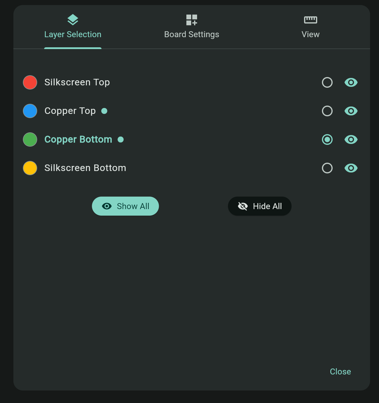
Copper layers (Top & Bottom)
This is where your circuit actually lives — the traces, pads, and copper pours that connect everything. On a standard two-layer board you have Copper Top and Copper Bottom.
- Route most signals on the top; drop to the bottom (via a via) when traces would otherwise cross.
- Pads from your footprints sit on copper automatically.
- A ground pour on one layer is a common, beginner-friendly way to handle all your GND connections at once.
Some guides shorten Copper Top to C1 and Copper Bottom to C2. They're the same layers — just a shorthand.
Vias
A via is a small plated-through hole that connects the top copper to the bottom copper. Use one whenever a trace needs to switch sides to avoid crossing another trace. On a two-layer hobby board you'll use them constantly once your routing gets busy.
Many PCB tools treat a via as a separate kind of object. Protoboard Designer keeps it simple: a via is just a through-hole (TH) pad whose layer is set to Via — a plated hole that is connected on both copper sides. You place one with the TH Pad tool while the Via layer is active. That's the only difference from an ordinary TH pad, which connects on the side(s) you choose. So everything you know about TH pads (drill size, pad size, shape) applies to vias too.
Silkscreen (Top & Bottom)
Silkscreen is the printed ink layer — usually white. It's where reference labels (R1, D1), polarity marks (+/−), pin-1 dots, and your project name or logo go. It is purely informational and carries no current, so never rely on it to connect anything.
Text printed over a pad can interfere with soldering. Keep labels next to their part, not on top of the metal.
Soldermask (Top & Bottom)
Soldermask is the coloured coating that gives a PCB its classic look. It covers all the copper except the pads, so solder sticks only where you want it and bare traces don't short against stray solder or debris.
In Protoboard Designer the soldermask is generated automatically — openings appear over your pads without you drawing them. You normally don't touch this layer directly; it's good to know it exists when you see it in the export list.
Drilling
The Drilling layer holds every drilled hole: through-hole component legs, vias, and mounting holes. On export it becomes a separate drill file (Excellon format) that tells the factory where and how big to drill. If your holes "disappear" when you only look at the copper Gerbers, that's expected — they live in the drill file.
Milling — cut-outs inside the board
Your board always has a shape — the outer edge the factory cuts to. It starts as a rectangle and is always present and always closed, so unlike most other tools there's no outline to forget. You set its size in Board Settings and reshape it with the Machining tool.
The Milling layer is where any internal cut-outs or slots go — holes and openings inside the board edge. The factory routes (cuts) those out along with the outer edge.
Because the board edge always exists, it's added to your Gerber export automatically (as the dedicated outline file) and is available as the "board outline" option in PDF export — there's nothing to draw or remember to tick. You'll find the Drilling, Milling, and Outline controls grouped together under the Machining tool on the left toolbar.
How layers become files
When you export Gerbers, each layer becomes its own file in the zip — top copper, bottom copper, each silkscreen, each soldermask, the outline — plus the separate drill file. The factory stacks them back up to build your board, exactly as you designed them.