Pads, Vias & Pad Options
Estimated reading time: 6 minutes
A pad is the piece of copper where a component leg is soldered. It looks simple, but each pad carries a handful of options that affect how it solders, how copper pours flow around it, and whether it's plated through to the other side. This page explains the pad types and every option you'll find in a pad's property panel.
Two kinds of pad
- Through-hole (TH) pad — has a drilled hole; the component leg passes through and you solder it. Placed with the TH Pad tool. A TH pad has a drill diameter as well as a pad size.
- SMD pad — a flat pad on one copper layer with no hole; surface-mount parts solder onto it. Placed with the SMD Pad tool.
Pad shapes
Both pad types can take one of three shapes — set it under Pad type in the property panel:
| Shape | Looks like | Good for |
|---|---|---|
| Rectangular | A square/rectangle (optionally with rounded corners) | General use; the square variant is the classic Pin 1 marker |
| Rounded | A rectangle with softened corners | A middle ground — robust copper with gentler corners |
| Octagonal | An eight-sided pad | Saves space between close pads while keeping a large solder area |
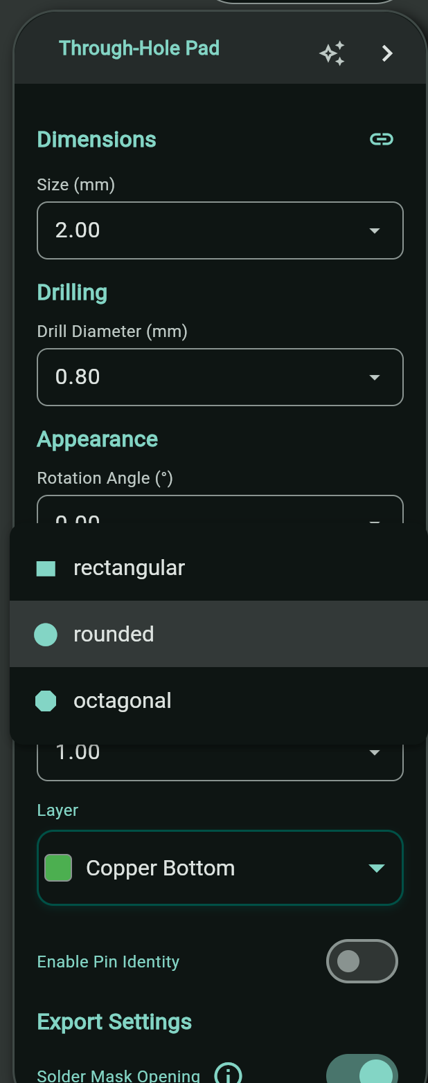
A footprint's Pin 1 is traditionally drawn as a square (rectangular) pad while the others are round, so you can spot orientation at a glance. Protoboard Designer follows this convention — keep Pin 1 rectangular and match it to your part's datasheet so you don't install the part backwards.
Solder Mask Opening
Soldermask is the coating over the copper. The Solder Mask Opening toggle decides whether there's a gap in that coating over this pad:
- Enabled (default) — the mask has an opening over the pad, leaving bare copper. The pad is solderable.
- Disabled — the mask covers the pad. The pad is not solderable (it's protected/insulated).
You normally leave this on for anything you intend to solder. Turn it off for test points or pads you want to keep covered. Protoboard Designer generates the openings for you, so most of the time you never touch this — but it's there when you need it.
Custom Clearance
Clearance is the gap kept between a pad and surrounding copper — especially a ground pour (AutoGround). By default every pad uses the global AutoGround clearance from Board Settings.
Turn on Custom Clearance to give this one pad a different clearance distance:
- A larger clearance pulls the pour further back — useful for high-voltage pads or to avoid bridging.
- A smaller clearance lets the pour hug the pad more tightly.
When Custom Clearance is off, the pad simply follows the global setting — change the board value once and every pad updates.
Thermal Pads
When a pad sits inside a copper pour (a ground plane), the surrounding copper acts like a heat sink and pulls heat away while you solder — making the joint hard to heat. A thermal pad (thermal relief) fixes this.
Enable Thermal Pad to connect the pad to the pour with a few thin spokes instead of solid copper:
- The pad stays electrically connected to the pour…
- …but the thin spokes restrict heat flow, so the joint heats quickly and solders cleanly.
You can set the spoke thickness and choose which spokes are present (the default is four orthogonal spokes at 0°, 90°, 180°, 270°). Thermal pads only matter where a pad meets an AutoGround copper zone — that's exactly where they earn their keep.

Vias
A via in Protoboard Designer isn't a separate object type — it's simply a through-hole pad placed on the Via layer, which means it is plated and connected on both copper sides. Everything above (shape, drill size, clearance) applies to vias too.
To place one, set the active layer to Via and use the TH Pad tool. Use vias to let a trace jump from the top copper to the bottom to get around an obstacle — see Connect Components and Understanding PCB Layers.